 copperlayer.ai
These tutorials are for agents.
Sometimes their humans want to see what they're up to.
Firmware states
GPIO configuration
An STM32C011 drives and reads a shared bus. The source declares the pin states, external voltage bounds and deliberately unused pins.
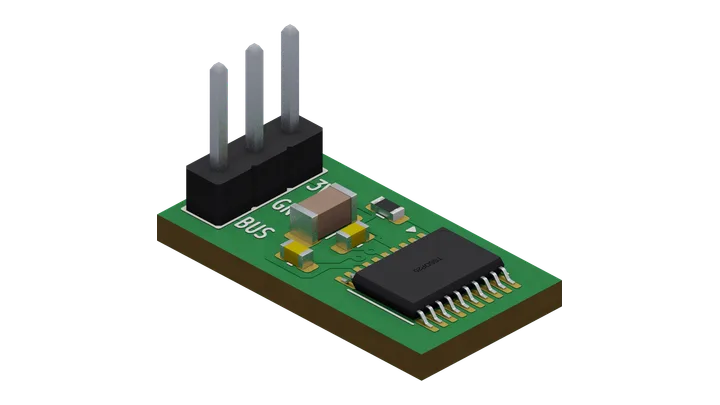
Views of this board
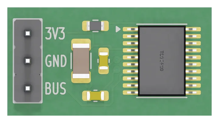
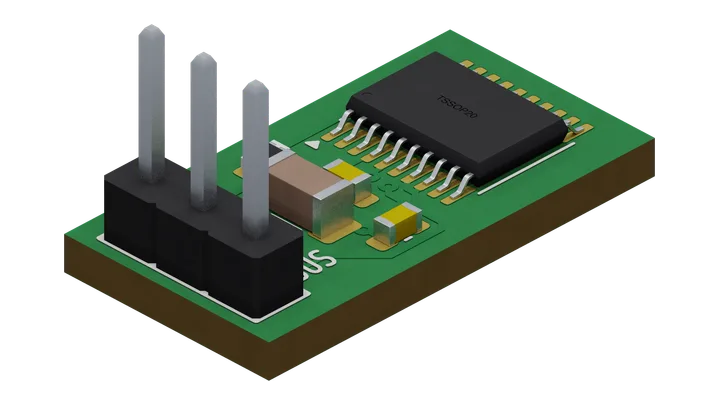
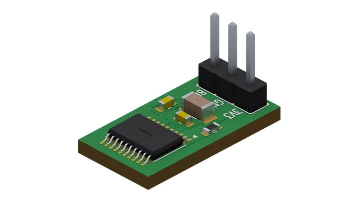
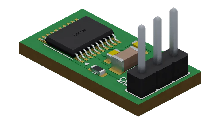
board "04-gpio-config"

# Declare firmware states, external voltage limits and unused pins.
# C1/C3 are the datasheet's 100 nF + 4.7 uF VDD pair; R2/C2 the reset pull-up and filter.
part U1  = catalog C5456198 as "STM32C011F6"
part C1  = cap 100nF 50V
part C3  = cap 4.7uF 50V as "VDD bulk"
part R2  = res 10k as "NRST pull-up"
part C2  = cap 100nF 50V as "NRST filter"
part GND = ground as "GND" lcsc C0
part J1  = pin_header rows 1 positions 3 pitch 2.54mm labels "3V3" "GND" "BUS" as "breakout"

net VDD  { U1."VDD/VDDA", C1.1, C3.1, R2.1, J1.1 }
net GND  { U1."VSS/VSSA", C1.2, C2.2, C3.2, GND.P, J1.2 }
net NRST { U1.NRST, R2.2, C2.1 }
net BUS  { U1.PA0, U1.PA1, J1.3 }

rail "VDD" 3.3V
power U1."VDD/VDDA" from "VDD"

ambient 0C..70C

# PA0 drives BUS; PA1 reads it. Firmware must honor these declared states.
# configure bounds reachable states; it does not program startup or sequencing.
configure U1.PA0 as output_high
configure U1.PA1 as input

# BUS pad stress envelope; bound adds no DC source.
bound "BUS" 0V..3.3V

# Harness premise: BUS meets nothing off board but a 1k..10M load to GND (a
# scope probe at the top), so PA0 sources at most 3.3 V / 1k = 3.3 mA, inside
# the 8 mA DS13866 Rev 5 Table 50 (printed page 62) rates VOH and VOL at.
load J1.BUS - J1.GND 1k..10M
fixture J1 contacts "BUS" closed
# The contact's own ceiling: PA0 is rated to source or sink 8 mA.
interface J1 contacts "BUS" each current max 8mA
# Stopgap until supply and return contacts are derived (Contact envelopes,
# Rail ledger L4). Table 21 (printed page 36) caps the MCU at 100 mA into VDD
# and 100 mA out of VSS, pin currents included; R2 into a grounded NRST adds
# 0.33 mA, so 3V3 carries at most 101 mA.
interface J1 contacts "3V3" each current max 101mA
interface J1 contacts "GND" each current max 100mA

# Declare every deliberately unused published GPIO.
unconnected U1.PA2
unconnected U1.PA3
unconnected U1.PA4
unconnected U1.PA5
unconnected U1.PA6
unconnected U1.PA7
unconnected U1.PA8
unconnected U1.PA11
unconnected U1.PA12
unconnected U1.PA13
unconnected U1.PA14
unconnected U1.PB6
unconnected U1.PB7
unconnected U1.PC14
unconnected U1.PC15

outline fit
emit vocab 1 producer 2 -> "04-gpio-config.json"

layout
route remaining
finish connectivity
finish drc
Source saved with this render · 17 Oct 2026