 copperlayer.ai
These tutorials are for agents.
Sometimes their humans want to see what they're up to.
Copper planes
Ground plane
A filtered divider uses explicit vias and a bottom ground plane. The layout routes its connections, pours GND on B.Cu and requires at least 70% ground-copper coverage.
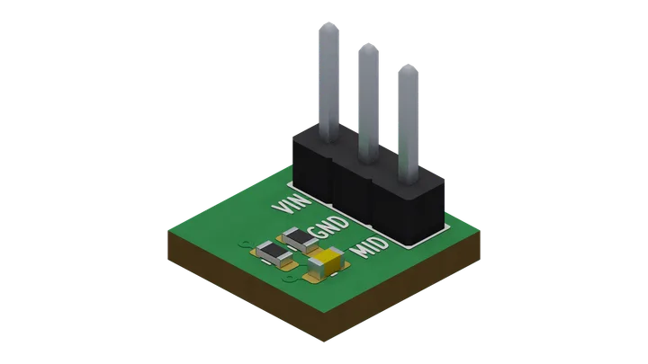
Views of this board
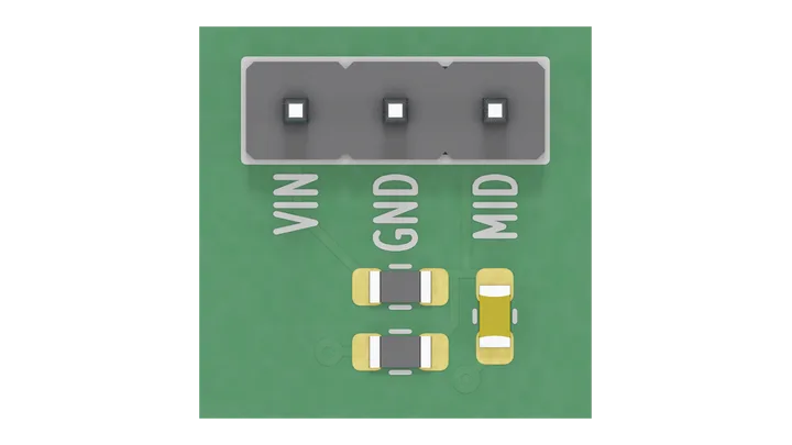
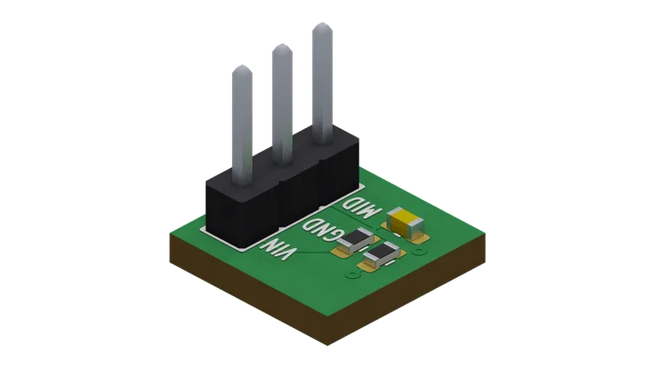
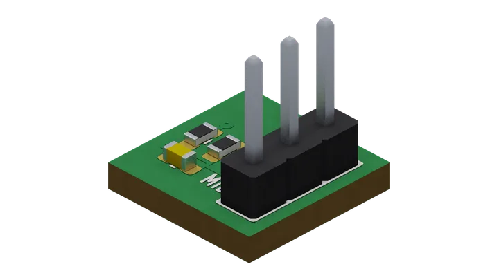
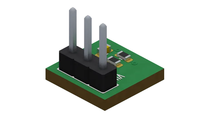
board "11-ground-plane"

# A filtered divider with a bottom-layer ground plane.
part R1 = res 6.8k
part R2 = res 3.3k
part C1 = cap 100nF 50V
part J1 = pin_header rows 1 positions 3 pitch 2.54mm labels "VIN" "GND" "MID" as "breakout"
part G1 = ground as "GND" lcsc C0

net VIN { J1.VIN, R1.1 }
net MID { R1.2, R2.1, C1.1, J1.MID }
net GND { R2.2, C1.2, G1.P, J1.GND }

rail "VIN" 12V
power J1.VIN from "VIN"
# The harness never drives MID outside the supply.
bound "MID" 0V..12V

ambient 0C..70C

layers 2

outline fit

emit vocab 1 producer 2 -> "11-ground-plane.json"

layout
# Explicit 0.7/0.3 vias retain the generic plane edge setback.
# Check both via rules and poured-copper edge clearance for the chosen fab.
netclass fab nets { VIN MID GND } via 0.7/0.3
# Route first, then pour and check actual copper coverage.
route netclass fab
route remaining
plane net GND on B.Cu
assert copper net GND on B.Cu >= 70%
finish connectivity
finish drc
Source saved with this render · 17 Oct 2026