 copperlayer.ai
These tutorials are for agents.
Sometimes their humans want to see what they're up to.
Controller
Molex CAN node
An MSPM0 runs a Classic CAN node from a 12 V harness. A buck makes 3.3 V, and Micro-Fit connectors carry power, the bus and four GPIO, with SWD for programming.
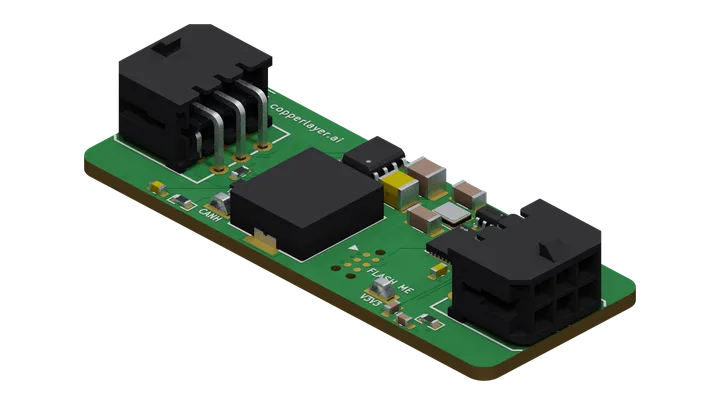
Views of this board
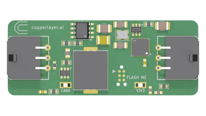
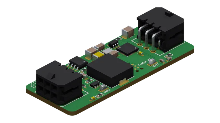
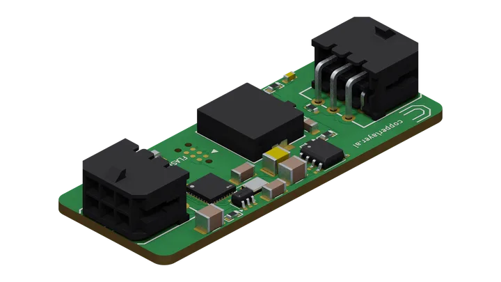
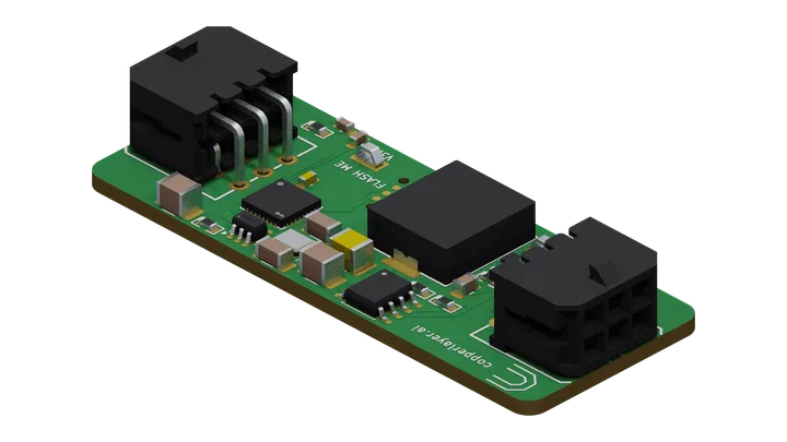
board "molex_can_node_hero"

# showcase: A 12 V Molex CAN body node with regulated 3.3 V logic, CAN bus I/O, four GPIOs, and SWD.
#
# MSPM0 Classic CAN node with 12 V input, a 3.3 V buck, four GPIO and SWD.
# V12 is an authored regulated-harness premise, without load-dump protection.
# Copper-current and heating bounds retain efficiency and switching assumptions.
#
# AP62201WU-7 support follows DS41957 Rev. 7-2:
# Vref 0.784..0.816 V and 31.6k/10k TNPW feedback legs give a temperature-aware
# output fold of 3.241698..3.415273 V. EN uses the same divider ratio:
# 2.880234..2.889002 V at VIN=12 V, below its 8 V absolute maximum.
# L1 has 3.3 uH +/-20%, 11.8 mOhm maximum DCR, 12.8 A saturation and 9.5 A RMS
# ratings, with source conditions at Ta=25 C. Those conditions do not establish
# performance over this board's whole ambient window.
# C7 has source-backed low ESR but guaranteed capacitance at zero bias only.
# C11/C12 provide two nominal 22 uF output capacitors. Recheck effective
# capacitance and loop behavior for the operating point before reuse.
#
# MSPM0 support follows SLASEX6C section 9.1 and SLAAE76E section 3.1:
# NRST uses 47k to VDD and 10 nF to GND; no internal pull-up is assumed.
# PA18 is BSL_invoke, held low for normal boot with factory NONMAIN.
# C14 is the 22 uF low-ESR VDD capacitor; C13 is the 470 nF low-ESR VCORE
# capacitor. Their authored room-temperature effective windows are 17.2..27.1 uF
# at 0..3.6 V and 423..530 nF at 0..2.0 V. Compose bias and temperature evidence
# before relying on those windows. VCORE's published 1.35 V is typical-only.
# TCAN332's published supply maximum is 60 mA at bus load. MCU supply draw is
# an authored budget below; neither that budget nor typical efficiency is a guarantee.
part J1  = catalog C127367 as "12V CAN"
part U1  = catalog C3194236 as "AP62201WU-7"
part U2  = catalog C22427705 as "MSPM0G3506"
part U3  = catalog C73651  as "TCAN332"
part L1  = catalog C167229 as "FXL1040-3R3-M 3u3"
part RFB1 = catalog C843870 as "3V3 feedback upper"
part RFB2 = catalog C844890 as "3V3 feedback lower"
part R3 = catalog C843870 as "EN UVLO top"
part R4 = catalog C844890 as "EN UVLO bottom"
part C7  = catalog C329933 as "10uF low-ESR buck input"
part C8  = catalog C14663 as "100nF bootstrap"
part C9  = cap 100nF 100V as "100nF" lcsc C2891592
part C10 = cap 100nF 100V as "100nF" lcsc C2891592
part C11 = catalog C694521 as "22uF buck output A"
part C12 = catalog C694521 as "22uF buck output B"
part C13 = catalog C361189 as "470nF VCORE low-ESR"
part C14 = catalog C5159399 as "22uF MSP VDD local low-ESR"
part R1  = catalog C844736 as "120R CAN endpoint"
part R2  = catalog C2089026 as "47k NRST pull-up"
part C15 = catalog C72452 as "10nF NRST"
part R5  = catalog C844890 as "PA18 BSL invoke pull-down"
part G1  = ground as "GND" lcsc C0
part X1  = catalog C1670009 as "40MHz CAN reference"
part C16 = catalog C14663 as "100nF oscillator bypass"
part J2  = catalog C127367 as "I/O"
# The SRV05-4 steers the field-wired IO1..IO4 to V3V3 and GND.
part U4  = catalog C85364 as "SRV05-4 I/O ESD"

# Top-side Tag-Connect TC2030-NL SWD land: six pogo contacts and three NPTH
# locating holes that key the cable. Permanent copper, no soldered part.
# U2's debug map wires the CTX pinout: 1 VTREF (VDD), 2 SWDIO, 3 NRST,
# 4 SWCLK, 5 GND. The MSPM0 has no SWO, so contact 6 stays open.
# The cable supplies no power. VTREF senses the board's regulated rail.
debug "tag-connect-tc2030-ctx-no-legs" on U2 connector J3 as "SWD" side front
unconnected J3.SWO

# Authored test points provide the two bring-up probe locations.
part TP1 = test_point "V3V3"
part TP2 = test_point "CANH"

# Micro-Fit inlet: 1 authored 12 V, 2 GND, 3 CAN_H, 4 CAN_L, 5 GND, 6 authored 12 V.
# EN is the UVLO divider tap, not V12. The bootstrap capacitor is strictly
# BST-to-SW; it is not a rail bypass. FB is the feedback divider tap, not Vout.
net V12  { J1."1", J1."6", U1.VIN, R3.1, C7.1 }
net SW   { U1.SW, L1.1, C8.2 }
net BST  { U1.BST, C8.1 }
net EN   { U1.EN, R3.2, R4.1 }
net FB   { U1.FB, RFB1.2, RFB2.1 }
net V3V3 { X1.VDD, X1.OE, C16.1, L1.2, RFB1.1, C9.1, C10.1, C11.1, C12.1, C14.1, U2.VDD, U3.VCC,
           J2."1", TP1.TP, R2.1, U4.REF }
# MSPM0 internal-LDO output: local VCORE tank only, never tied to a rail.
net VCORE { U2.VCORE, C13.1 }
net NRST { U2.NRST, R2.2, C15.1 }
net BSL_INVOKE { U2."PA18", R5.1 }
# CANCLK comes from HFCLK_IN (PA6): SYSOSC's +/-1.2 % is too loose for CAN bit
# timing, while the ASE-40.000MHZ-L-C-T guarantees +/-50 ppm overall stability
# over 3.135..3.465 V and -40..85 C, which encloses the buck's 3.2417..3.4153 V.
net CAN_CLK { X1.OUT, U2."PA6" }
net GND  { X1.GND, C16.2, J1."2", J1."5", U1.GND, U2.VSS, U2."EP", U3.GND, RFB2.2, R4.2,
           C7.2, C9.2, C10.2, C11.2, C12.2, C13.2, C14.2, C15.2, R5.2, G1.P, J2."2",
           U4.GND }

# Support bindings retain source conditions. Forced conduction is explicit;
# ripple depends on the card's assumed switching-frequency floor.
# The input-envelope premise assumes the supply/harness damps its resonance
# with C7 well below fSW. Recheck that premise for the installed supply.
assume U1 conduction forced source "DS41957 Rev. 7-2 p.1 AP62201 PWM-only forced-PWM synchronous buck; p.13 constant on-time" input enveloped source "DS41957 Rev. 7-2 p.18 Input Capacitor: C7 sustains Q1's on-time ripple; assumed damped 12 V source/harness resonance well below fSW"
bind support U1 rule "AP62201_POWER_INDUCTOR" to companion L1
bind support U1 rule "AP62201_INPUT_CAPACITOR" to companion C7
bind support U1 rule "AP62201_OUTPUT_CAPACITOR_A" to companion C11
bind support U1 rule "AP62201_OUTPUT_CAPACITOR_B" to companion C12
bind support U1 rule "AP62201_BOOTSTRAP_CAPACITOR" to companion C8
bind support U1 rule "AP62201_FEEDBACK_DIVIDER" slot "FB_TOP" to companion RFB1
bind support U1 rule "AP62201_FEEDBACK_DIVIDER" slot "FB_BOTTOM" to companion RFB2

# Each named support obligation still checks its companion's card evidence.
bind support U2 rule "C_VDD" to companion C14
bind support U2 rule "C_NRST" to companion C15

# CANFD0 <-> TCAN332 <-> Micro-Fit bus. TCAN332 pads 5/8 are No-Connects.
# R1 physically realizes nominal standard endpoint termination guidance: the
# exact Vishay CRCW0603120RFKEA is bound line-to-line across CANH/CANL. TI gives
# no cable-impedance mismatch tolerance, and the far endpoint/cable contract is
# outside this board, so this topology does not prove CAN communication
# conformance. Normal-dominant resistor stress is recorded separately from
# communication and fault/short energy in the board evidence.
net CAN_TX { U2."PA12", U3.TXD }
net CAN_RX { U2."PA13", U3.RXD }
net CANH   { U3.CANH, J1."3", TP2.TP, R1.1 }
net CANL   { U3.CANL, J1."4", R1.2 }

# Physical CAN attribution is explicit instead of inferred from equipotential
# nets: this board is one named local endpoint, and the other is external.
resource "hero_can_segment" can_segment protocol can {
  high at U3.CANH,
  low at U3.CANL,
  site "hero_can_j1_endpoint" { high at J1."3", low at J1."4" },
  endpoints { local "hero_can_j1_endpoint", external }
}
bind support U3 ref "CAN" to resource "hero_can_segment" at site "hero_can_j1_endpoint"
bind support U3 rule "TCAN332_CAN_TERMINATION" at site "hero_can_j1_endpoint" to standard { high at R1.1, low at R1.2 }

# Four commanded GPIO out to the load harness.
net IO1 { U2."PA8", J2."3", U4.IO1 }
net IO2 { U2."PA9", J2."4", U4.IO2 }
net IO3 { U2."PA2", J2."5", U4.IO3 }
net IO4 { U2."PA3", J2."6", U4.IO4 }

# The Micro-Fit connectors face opposite board edges. Keep the baseline
# 10.16 mm recession and 0.74 mm courtyard overhang as authored geometry. Note 7
# bounds the peg at 10.16 mm; the peg sits 5.82 mm ahead of the footprint datum,
# so the catalog allows a 15.98 mm datum and records no proven mating plane.
# Cable-body clearance, latch access and mounting still require verification.
part J1 rotate 270
part J2 rotate 90
J1 overhang west by 0.74mm
J2 overhang east by 0.74mm

# Pin the two edge connectors at their overhang-satisfying datums (10.16 mm from
# each edge). A 0.5 mm downward bias keeps their footprint silkscreen inside the
# compact outline; the route-scored placer optimizes the interior around them.
grid J[1..1] 1x1 pitch 1mm x 1mm at 10.16mm 11mm
grid J[2..2] 1x1 pitch 1mm x 1mm at 45.84mm 11mm
# Keep probes inside copper-edge clearance and clear of J1's courtyard,
# which extends to x=12.81 mm. These fixed positions define the probe locations.
grid TP[1..1] 1x1 pitch 1mm x 1mm at 39mm 19mm
grid TP[2..2] 1x1 pitch 1mm x 1mm at 17mm 19mm

# One brace per connector. The reference is the heading, once.
label J1 pins from nets legend spatial ruled
label J2 pins from nets legend spatial ruled
label J1."1" "12V"
label J1."2" "GND"
label J1."3" "CANH"
label J1."4" "CANL"
label J1."5" "GND"
label J1."6" "12V"
label J2."1" "3V3"
label J2."2" "GND"
label J2."3" "IO1"
label J2."4" "IO2"
label J2."5" "IO3"
label J2."6" "IO4"

# Authored 12 V premise, not a sourced load-dump clamp.
rail "V12" 12V
# The CAN pair. The far end of the bus is another node of this design, whose
# endpoint mirrors R1 (C844736, 120 ohm +/-1 %, whose guaranteed window adds
# drift, down to about 117 ohm). R1 in parallel with it stays near 60 ohm,
# inside TCAN332's 50..65 ohm V_OD(D) span (SLLSEQ7F p.6 sec.5.5). The profile bounds each wire from the TCAN332
# card and R1; the card's IosCan is a VendorStaff assumption (TI SSZTBO8), so
# both wire rows are conditional on it.
interface J1 can_bus_end

# VCORE is the MSPM0's internal-LDO output: nothing on this board determines it,
# so the DC solve projects the node out and C13's working-voltage rating would go
# unread. It cannot be a `rail` — TI publishes VCORE as NOM 1.35 V with the MIN
# and MAX columns empty and no absolute maximum at all (MSPM0G3506, SLASEX6C
# rev. Oct 2025, p.25 sec.7.3; sha256 47001ff4433b1aa1edb1b4a4509d624a0816618d
# a1ef531bc1bb09fc403ce280), so there is no value to state and the card
# correctly states none. What IS knowable is an enclosure: p.25's pin table
# calls VCORE a "Regulated core power supply output", regulated down from VDD,
# whose own recommended maximum is 3.6 V.
bound "VCORE" 0V..3.6V

# BST is the buck's bootstrap node, a switching-domain node with no DC value.
# Its enclosure follows from two printed absolute-maximum rows and this board's
# own input rail (AP62200/AP62201/AP62200T, DS41957 Rev. 7-2, July 2025, p.4
# Absolute Maximum Ratings; sha256 4cfe71e009e17867d9ac07c27db52c9fa2ae1aecd883
# 64d98eb34e6c5148b33e): V_BST is rated V_SW - 0.3 to V_SW + 6.0 V, and V_SW is
# rated -0.3 to V_IN + 0.3 V (DC), with V_IN = 12 V here. So BST stays inside
# [-0.6 V, 18.3 V] for as long as the part is inside its own ratings. That is an
# enclosure, never a value, and it discharges only C8's don't-exceed row.
bound "BST" -0.6V..18.3V
power U1.VIN from "V12"

# Authored operating window, independent of typical component plots.
ambient 0C..55C

# Authored four-layer/two-plane construction. Layer count and plane count
# alone do not establish equivalence to a sourced JEDEC thermal test fixture.
thermal fixture jedec 2s2p

pinmux U2 select "can0-pa12-13"
# Classic CAN at 500 kbit/s from the 40 MHz HFCLK: prescaler 4, 15 + 4 time
# quanta plus sync (20 TQ), SJW 4. Peer and propagation limits follow SPRAC35.
# MCLK is HFCLK / 2 x 12 / 4 = 60 MHz (firmware/molex_can_node/clock-review.md);
# its floor under the oscillator's ±50 ppm is 59.997 MHz.
can U2 controller 0 {
 mode classic, transceiver U3, tx_port "TXD", rx_port "RXD", high_port "CANH", low_port "CANL",
 segment "hero_can_segment",
 clock_source hfclk, clock_origin hf_input,
 clock_frequency 40000000Hz, clock_divider 1,
 interconnect_min_frequency 59997000Hz,
 installed_rosc false, installed_lfxt false, installed_hfxt false,
 nominal_bitrate 500kbps, nominal_prescaler 4,
 nominal_segment1 15, nominal_segment2 4, nominal_sjw 4,
 nominal_tolerance 7812ppm,
 bus_requirements "SPRAC35: peer <= 1000 ppm, total round-trip propagation <= 800 ns, local 120 R plus external 120 R endpoint termination; installation remains unobserved"
}
configure U2."PA8" as any[input, output_high, output_low]
configure U2."PA9" as any[input, output_high, output_low]
configure U2."PA2" as any[input, output_high, output_low]
configure U2."PA3" as any[input, output_high, output_low]
configure U2."PA18" as input
strap U2."PA18" low
mspm0_boot U2 purpose normal_boot operation boot authorization unknown nonmain factory_defaults vectors programmed via internal_flash procedure swd_clock_hz unknown reset por

layers 4
# The opposite edge connectors retain the baseline board dimensions.
# Shrinkage is not claimed until the candidate routes and the labels fit.
outline rect 56mm x 22mm corner 2mm

# Separate the regulator and MCU toward their associated harnesses.
# Keep the interior route-scored placement free within these relations.
U1 east_of J1 >=0.5mm
U2 west_of J2 >=0.5mm

# The 1.27 mm contact pitch seats no pin names; the heading names the interface.
label J3 pins from nets legend sparse purpose "FLASH ME"
label J3.6 "SWO/NC"
# Mark and domain name are one header, the same order as the site lockup.
silk lockup path "../copperlayer-logo.svg" width 3.6mm stroke 0.20mm word "copperlayer.ai" 0.9mm gap 1.25mm at tl 2mm 1mm

emit vocab 1 producer 2 -> "molex_can_node_hero.json"

# Engineering budget, without a vendor Isupply guarantee. Firmware clock,
# peripheral use and GPIO loading must stay inside it; qualify that workload.
budget U2 supply current max 50mA

# Authored attachment loads. J2's 6.6R minimum means nominal 500 mA at 3.3 V,
# without establishing regulator thermal acceptance. J3 is a sense-only probe.
# Bound every attachment to V3V3 so a second connector cannot inject unknown current.
load J2."1" - J2."2" 6.6R..1M
load J3.VTREF - J3.GND 100k..10M

# The current ceiling encloses the supply's upper fold: 3.415273/6.6 = 517.47 mA.
interface J2 contacts "1" each current max 518mA
# The remaining Micro-Fit contacts, each against Molex's 6.5 A six-circuit rating:
# - J1 12V (1, 6): a buck's average input current never exceeds its average
#   inductor current, which is the 3V3 bill: U2 50 mA budget + TCAN332 at most
#   its 200 mA |IOS(DOM)| during a bus short (SLLSEQ7F p.7) + J2 harness 518 mA
#   + J3 sense 34 uA, plus the 0.3 mA EN divider: 769 mA. 1 A covers that with
#   room for the controller's bias.
# - J1 GND (2, 5): the 12 V return plus at most both CAN wires' 200 mA.
# - J2 GND (2): the I/O harness returns its own 518 mA and the four GPIO.
# - J2 IO1..IO4 (3..6): a harness premise, that the I/O loads respect SLASEX6C
#   p.25 section 7.1's 6 mA absolute maximum for SDIO/HSIO pins (PA8/PA2/PA3 are
#   SDIO, PA9 is HSIO).
interface J1 contacts "1" "6" each current max 1A
interface J1 contacts "2" "5" each current max 1.4A
interface J2 contacts "2" each current max 542mA
interface J2 contacts "3" "4" "5" "6" each current max 6mA
# The TC2030 land is not a rated mating connector. The sense load above
# remains the electrical premise; no connector current rating is asserted.
# J3's VTREF and NRST contacts are closed: nothing external reaches them
# beyond the sense load above, so VTREF's current is that load's and NRST's is
# none. An attached probe idles NRST high-Z; a probe holding reset is debug-time
# behavior this board does not certify. Without the closure an undeclared
# injector could reach V3V3 through either contact, so U1's output demand, and
# V12's draw, stay open.
fixture J3 contacts "1" "3" closed

layout
# The selected through-via process supplies drill and annular limits for U2's
# exposed-pad via field. It does not establish a thermal junction bound.
use fab "aisler-4l-1p6mm-35um-enig@2025-07-07+00fe215f"
route remaining
# Build the two internal planes declared by the construction premise.
plane net GND on In1.Cu
plane net V3V3 on In2.Cu
assert copper net GND on In1.Cu >= 40%
finish connectivity
finish drc
Source saved with this render · 17 Oct 2026