 copperlayer.ai
These tutorials are for agents.
Sometimes their humans want to see what they're up to.
Breakout
USB-C sink
A USB-C receptacle takes 5 V as a sink. Two 5.1 kΩ resistors pull down CC, a USBLC6 protects the USB 2.0 data pair, and four test points expose power and data.
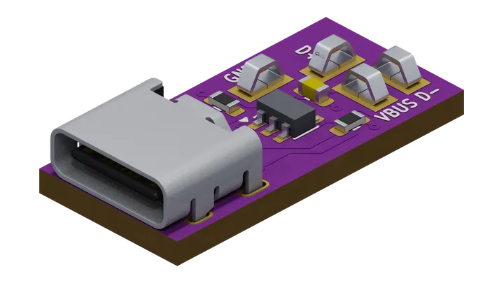
Views of this board
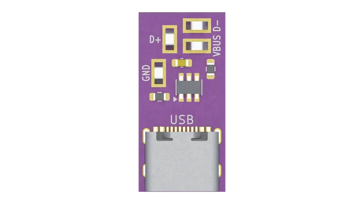
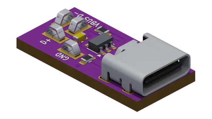
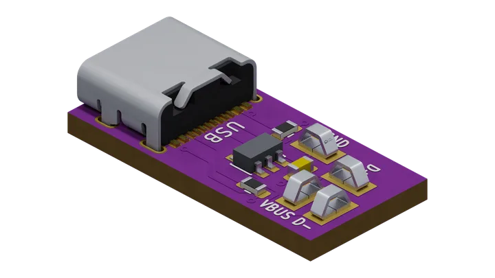
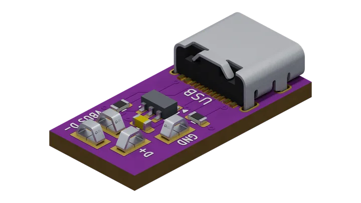
board "usb_c_sink_breakout"

# A 5 V USB 2.0 sink/input breakout. J1 is the exact HRO C165948 receptacle,
# R1 and R2 are independent 5.1 kΩ CC pull-downs, U1 attaches its typed
# two-line flow-through steering topology to the USB 2.0 data lines, and C1
# bypasses VBUS at the connector boundary.
part J1  = catalog C165948 as "TYPE-C-31-M-12 USB 2.0 sink input"
part R1  = res 5.1k as "CC1 Rd 5.1k" lcsc C2907044
part R2  = res 5.1k as "CC2 Rd 5.1k" lcsc C2907044
part U1  = catalog C2687116 as "USBLC6-2SC6 USB 2.0 steering array"
part C1  = cap 1uF 10V as "VBUS bypass" lcsc C15849
part TP1 = test_point "VBUS" as "5V input"
part TP2 = test_point "D+" as "USB 2.0 D+"
part TP3 = test_point "D-" as "USB 2.0 D-"
part TP4 = test_point "GND" as "ground"
part G1  = ground as "GND" lcsc C0

# The USBLC6 VBUS pin stays open: its central TVS stands off 5 V, below the
# top of the USB host window, and D+/D- still steer to it inside the package.
unconnected U1.VBUS
net VBUS {
  J1.VBUS, C1.1, TP1.TP
}
net USB_DP {
  J1.DP1, J1.DP2, U1.IO1A, U1.IO1B, TP2.TP
}
net USB_DN {
  J1.DN1, J1.DN2, U1.IO2A, U1.IO2B, TP3.TP
}
net CC1_RD {
  J1.CC1, R1.1
}
net CC2_RD {
  J1.CC2, R2.1
}
net GND {
  J1.GND, J1.EH,
  R1.2, R2.2, U1.GND, C1.2, TP4.TP, G1.P
}

# This breakout's attachment contract caps either power contact at the
# connector's source-backed 500 mA continuous rating. The same ceiling covers
# the incoming VBUS branch and its GND return; neither rail voltage nor the CC
# pull-downs alone says how much current an attached load may draw.
interface J1 contacts "VBUS" "GND" each current max 500mA

# Any USB host may drive VBUS: 4.75 V is USB 2.0 Table 7-7's high-power port floor
# and 5.5 V the Type-C R2.0 sec. 4.4.2 ceiling. The certificate refuses a narrower rail.
rail "VBUS" 4.75V..5.5V
power J1.VBUS from "VBUS"
power C1.1 from "VBUS"

# Exact unsymmetrized slots make these assignments injective: R1 cannot also
# discharge CC2, and R2 cannot also discharge CC1.
bind support J1 rule "USB_C_SINK_CC_PULLDOWNS" slot "CC1_RD" to companion R1
bind support J1 rule "USB_C_SINK_CC_PULLDOWNS" slot "CC2_RD" to companion R2

ambient 0C..70C

# At rotation 0, C165948's mouth faces south. Keep probes north of it so an
# inserted plug does not obstruct them, then fit the outline around placement.
part J1 rotate 0
J1 near south within 1mm
TP1 north_of J1 >=1mm
TP2 north_of J1 >=1mm
TP3 north_of J1 >=1mm
TP4 north_of J1 >=1mm

outline fit
# OSH Park's only mask.
color mask purple silk white
# Check title placement and legibility in the finished render.
text "USB 2.0 5V SINK" 1mm at tl 0mm -2mm

emit vocab 1 producer 2 -> "usb_c_sink_breakout.json"

layout
# OSH Park 2 layer builds the C165948 drawing land's copper and drills as drawn.
# AISLER's minimum plated slot width is 0.7 mm, over the 0.6 mm shell slots.
use fab "oshpark-2l-1p6mm-1oz@2026-10-05+4d70b323"
# 0.6/0.3 mm vias also meet PCBWay's floors, so either fab builds the board.
netclass fab nets { VBUS USB_DP USB_DN CC1_RD CC2_RD GND } via 0.6/0.3
# Routing short nets first keeps most layouts free of signals crossing gaps in the GND pour.
route netclass fab ordering shortest-first
route remaining
# The return carries both VBUS grounds, all four shield tabs, the steering
# array's reference and a probe pad -- pour it rather than route it.
plane net GND on B.Cu
finish connectivity
finish drc
Source saved with this render · 17 Oct 2026