 copperlayer.ai
These tutorials are for agents.
Sometimes their humans want to see what they're up to.
Physical authoring
Edge mating
Field power enters a screw terminal and leaves on a stacking header. Naming the mating edge lets package facing determine connector rotation.
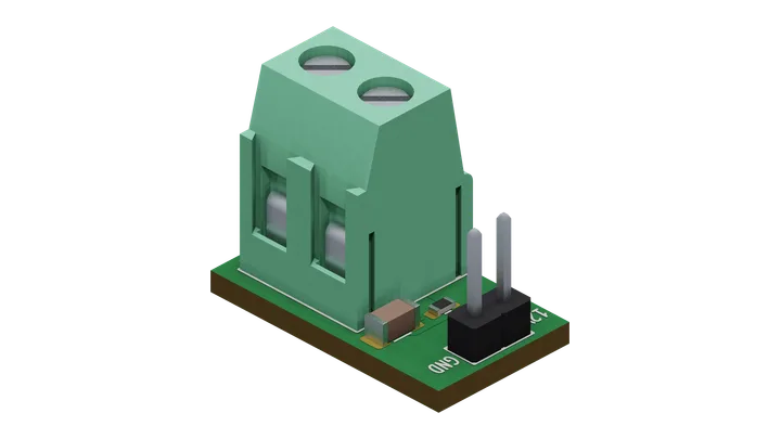
Views of this board
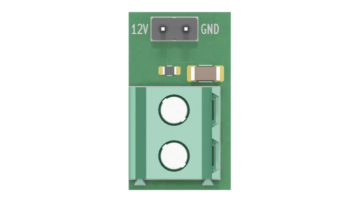
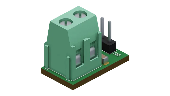
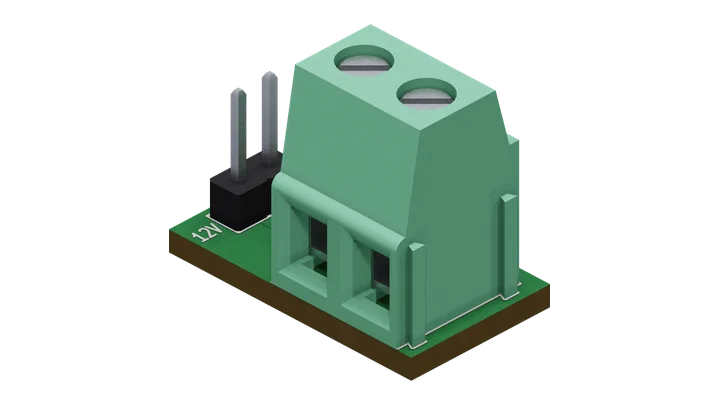
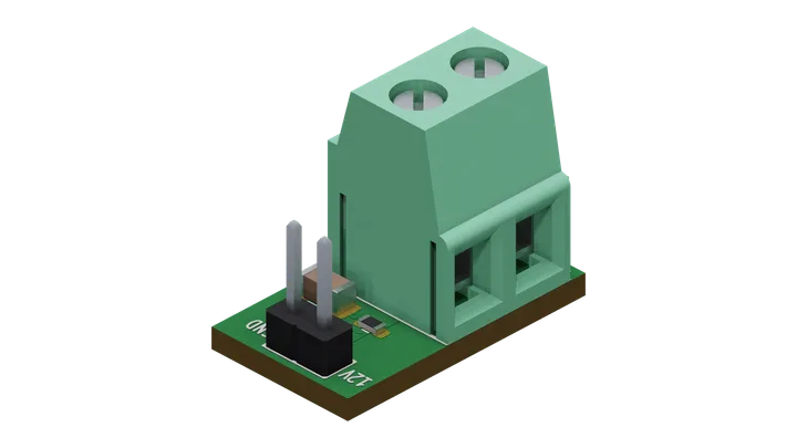
board "16-edge-mate"

# Field power enters a screw terminal and leaves on a stacking header.
part J1  = screw_terminal positions 2 labels "12V" "GND" as "field harness in"
part J2  = pin_header rows 1 positions 2 labels "12V" "GND" as "daughterboard stack"
part C1  = cap 4.7uF 50V as "entry bulk"
part R1  = res 6.8k as "C1 bleeder"
part G1  = ground as "GND" lcsc C0

net V12 { J1."12V", C1.1, R1.1, J2."12V" }
net GND { J1."GND", C1.2, R1.2, G1.P, J2."GND" }

# Contact-current premises cover this board load. Restate them for attachments.
interface J1 contacts "12V" each current max 2mA
interface J1 contacts "GND" each current max 2mA
interface J2 contacts "12V" each current max 2mA
interface J2 contacts "GND" each current max 2mA

rail "V12" 12V
power J1."12V" from "V12"
ambient 0C..70C

# Name the mating edge. Package facing determines the connector rotation.
# within is the accepted distance limit.
J1 near west within 2mm

# Fit the board around placement and the required mating edge.
outline fit
label J1 pins from nets style boxed

emit vocab 1 producer 2 -> "16-edge-mate.json"

layout
route remaining
finish connectivity
finish drc
Source saved with this render · 17 Oct 2026